
When building fuzz and overdrive pedals, proper transistor biasing is key to getting the tone, sustain, and response just right. The bias calculators help you set the correct DC operating point for each transistor stage so that your circuit behaves consistently and sounds its best.
Using the Bias Calculators for Fuzz and Overdrive Circuits
Select the transistor type – Choose whether you’re biasing a silicon or germanium transistor. The calculator uses typical forward-voltage values for each type.
Enter your supply voltage (VCC) – Most classic fuzz circuits run on 9V, but you can adjust this to match your build.
Adjust resistor values – Input your collector, base, and emitter resistor values (or potentiometer positions) to see how they affect collector voltage and current.
Aim for the sweet spot – For a traditional two-transistor Fuzz Face or Tone Bender, the collector voltage of the second transistor should typically fall around 4.5 V (half the supply voltage). This centers the signal swing and gives a warm, smooth distortion instead of gated or splattery output (unless that is what you are into).
Experiment and fine-tune: Small resistor changes can drastically alter tone. Use the calculator to preview how bias shifts impact gain, headroom, and clipping symmetry before soldering or swapping parts.
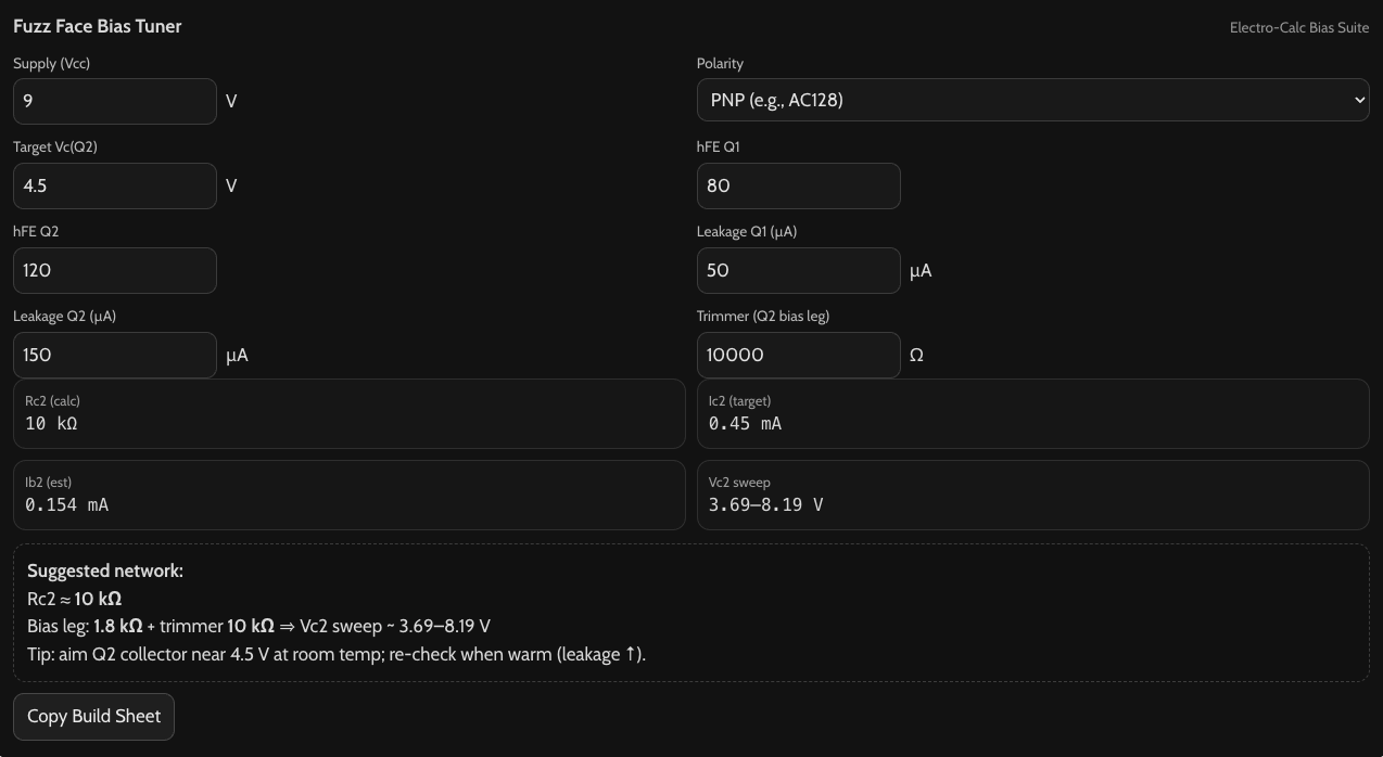
Fuzz Face Bias Helper
In a traditional germanium Fuzz Face (using transistors like AC128, NKT275, or 2N404/mp16b), both bias voltage and transistor gain (hFE) determine how smooth or wild the fuzz will sound.
1. Choose transistors with proper hFE:
- Q1: lower gain, around 70–90 hFE
- Q2: higher gain, around 100–130 hFE
This pairing keeps noise low while allowing Q2 to saturate smoothly. If hFE is too high, you’ll get harsh, oscillating fuzz. Too low, and it will sound gated or weak.
2. Set your bias values:
- VCC: 9 V
- Collector resistor (RC): 8.2 kΩ
- Base resistor (RB): 33 kΩ
- Emitter resistor (RE): 470 Ω
Using the bias calculator, adjust these values until Q2’s collector voltage (VC) is roughly 4.5 V — that’s the sweet spot for classic, dynamic response.
3. Fine-tune by ear and meter:
- Measure hFE for each transistor (most DMMs have a transistor socket).
- Use the calculator to simulate how each device’s gain affects bias current and collector voltage.
- Swap or re-bias until Q2 sits comfortably near half the supply voltage under load.
Why hFE matters:
Finding the exact right transistors for a schematic is tough work. Matching hFE ranges between Q1 and Q2 creates the right mix of cleanup ability (when you roll back the guitar volume) and rich saturation when maxed out.
BJT Bias Helper
JFET Bias Helper
JFETs (Junction Field-Effect Transistors) are prized in audio work for their smooth, tube-like clipping and dynamic response. They’re common in preamp stages, buffers, and amp-style overdrive pedals. The JFET Bias Calculator helps you set the drain current (ID) and drain voltage (VD) so the device operates in its most linear region — giving you consistent tone and predictable gain.
1. Understand JFET biasing basics:
Unlike bipolar transistors, JFETs are voltage-controlled. Their current is set by the voltage difference between gate and source (VGS). Each device has its own IDSS (maximum drain current when VGS = 0) and VGS(off) (pinch-off voltage). These vary widely, even among identical part numbers.
Measuring IDSS and VGS(off) for Your JFETs
Because JFETs vary widely from one device to another, even within the same part number, measuring IDSS and VGS(off) ensures your bias calculator results are accurate and your circuit behaves consistently.
1. What You’ll Need
- A 9 V battery or low-voltage DC supply (5–9 V is fine)
- A digital multimeter (DMM) that can measure milliamps and volts
- A breadboard or clip leads
- One resistor (around 1 MΩ)
2. Measuring IDSS (Drain current at VGS = 0 V)
This shows the JFET’s maximum current flow when the gate is shorted to the source.
Steps:
- Connect gate directly to source (short them together).
- Connect the drain through your ammeter to +9 V.
- Connect the source to ground.
- Power up and note the current (in mA) — that’s IDSS.
(Example: a J201 might measure 0.7 mA.)
3. Measuring VGS(off) (Pinch-off voltage)
This is the negative gate-to-source voltage where the JFET nearly stops conducting.
Steps:
- Keep the drain connected to +9 V through a 10 kΩ resistor.
- Connect the source to ground through your DMM (set to measure voltage).
- Slowly apply a negative voltage (or reverse the battery leads) between gate and source until the drain current nearly stops flowing (near 0 mA).
- The gate-to-source voltage at that point is VGS(off) (usually between –0.3 V and –4 V for small-signal JFETs).
(Example: your J201 might measure –1.1 V.)
4. Input These Values
Once you’ve recorded IDSS and VGS(off), plug them into the JFET Bias Calculator.
The calculator uses these to estimate the correct source resistor (R_S) and drain resistor (R_D) for your supply voltage, targeting a drain voltage around half of VCC for clean headroom and balanced tone.
2. Enter your JFET parameters:
- IDSS (mA): the current at VGS = 0 V
- VGS(off) (V): the negative gate-to-source voltage where the JFET stops conducting
These two values are often listed in the datasheet (e.g., for J201: IDSS ≈ 0.6–1.0 mA, VGS(off) ≈ –0.3 to –1.5 V).
3. Target the midpoint bias:
Use the calculator to find resistor values (R_D and R_S) that place VD at about ½ VCC. This centers the signal swing for clean headroom and low distortion.
- Too low a VD: mushy, compressed, and early clipping.
- Too high a VD: brittle tone and low gain.
4. Fine-tune by ear:
JFETs vary device-to-device; even parts from the same batch need slightly different source resistors. The calculator gives a solid starting point, but don’t hesitate to tweak R_S (source resistor) until it sounds right.
Example:
For a J201 running on 9 V with IDSS = 0.8 mA and VGS(off) = –1.0 V, bias for VD ≈ 4.5 V. The calculator might suggest R_D ≈ 22 kΩ and R_S ≈ 2.7 kΩ — a balanced point for clean, amp-like tone.